Products & Services

We strive to deliver your project on time and on budget with the highest level of quality.
Changing The Tides of Technology

Why Choose Our Services?

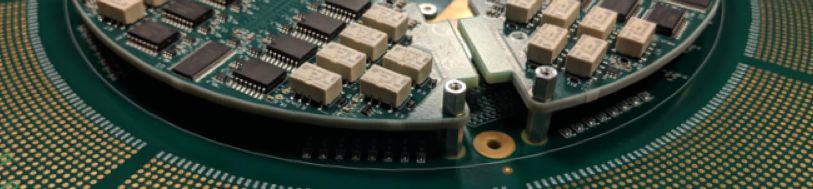
In addition to our skilled and experienced team of engineers, We differentiate ourselves with our approach to customer satisfaction, project management, regular communication, check-steps and our focus on design for manufacturability.  Our process is to listen to your challenges and offer across the spectrum solutions including a superior layout PCB mother board, specialized pitch translation, custom modules and instrument extensions.  We will offer the most effective solution available to solve your test interface challenges.  The NextWave team strives to deliver your project on time and on budget with the highest level of quality expected.

Hardware Interface Engineering

PCB Board, Load Board and Interface Design
NextWave 360 uses most of the available design software packages available. Please check with us for compatibility. We offer database creation, component library creation, schematic capture, PCB component placement & layout & documentation. We will review each milestone with you as needed before proceeding. We have a quality control organization that reviews all designs internally for accuracy as well as a customer review to gain approval for FAB release. Our designs are also reviewed by FAB engineers to ensure design for manufacturing requirements have been met prior to release. Our quality control design check steps will ensure a first run FAB yield and a properly functioning board upon arrival.
Instrument Extensions & Z-Factor Modules
A circuit board designed to provide test capability that the current tester does not have. A tester instrument's functions may need to be expanded to enhance measurement resolution, speed, or current delivery. This can be accomplished by a series of modules and/or PCB's located either in the tester or on the load board. This is a custom design service that we offer.
Fabrication
NextWave 360 is a full turnkey hardware interface solution company, with our own internal PCB FAB. Our strong PCB design team works directly with customers to verify design accuracy and signal integrity before releasing to FAB. Our team also has the ability to work directly with our internal FAB to ensure that all design for manufacturing requirements are met. Upon customer design approval and meeting our FAB quality check steps, the project will be released. Our internal processes help control your costs by producing high output yield, and the assurance that your PCB will function as designed upon arrival. Since we are not a fabless company, we are not passing on any additional markups to your project. We also offer design simulation services as needed and requested.
Assembly
As part of our full turnkey product delivery services, we include full assembly of your PCB boards. We take ownership of the entire process from identifying and procuring components to the final testing of the board. We know that long lead time components can lead to missed deadlines and project schedule slips. We are active in this through the design process and our technical experts will work with you to suggest alternative components as needed. We have capability for both hand assembly and reflow, pick and place assembly. We also provide 3D-AOI, and X-Ray review through the process and Flying Probe if requested.
Tester Platforms
We can work with the installed base of most tester platforms in the field. If a platform is new to us, we can work with you to setup the databases and artwork to proceed with a design solution for you.

Innovative Solutions

Test Enhancement Modules
Modules designed as part of interface connectivity that enhances the testers capabilities, thus expanding the tester’s current capability further and expanding the life of the tester before the customer would need to upgrade.  The modules allow customer to reach cost down goals through test time reduction, increased site count or simply increasing the amount of available application space on the load board.
Interposers
Micro-scale PCB's to translate ultra-fine-pitch DUT pin arrays to be in alignment with typical DIB-scale DFM parametric. Advanced manufacturing techniques are used in creating a monolithic space transforming solution that exceeds current capabilities in a more reliable and cost-effective package. The ability to transform a 0.25mm WLCSP footprint to that of a 0.65mm pitch device takes enough of a burden off the main DIB design that the complexity of interfacing such a device to a DIB becomes a mere afterthought. The capability of creating a coaxial via path unlocks even the most intriguing of doors.