Interface Modules & Instrument Extensions
In today’s test environment, site counts, pin counts and resource demands of testers are ever increasing, yet few investments are being made to increase overall applications space and loadboard size. These demands present a major challenge to PCB designers: “jam more stuff in smaller spaces”. It is true that a few platforms are seeing increased loadboard applications areas, but with the increase of signal speeds and demands of high-performance instruments – “bigger is not always better”. PMIC/Automotive devices do not want their current-switching relays in the nether regions of the DIB just the same as RF transceivers do not want tuning circuitry competing with relay pins in the DUT area because there is no other option for relays on your 32 Site DIB.
It’s time to start thinking of an “upper deck” solution in the DUT area in particular. Most applications and test engineers have dreaded modularization of DIB circuitry due to poor mechanical and electrical performance of interconnect solutions. We at NextWave360 recognize these concerns and have overcome them by selecting state-of-the art interconnects from Samtech that deliver speeds up to 56 GBPS while offering in excess of 1A per pin. Our modules (Z-Factor Product Line) also allow for the integration of simple, yet highly-effective stiffeners, enclosures and stand-offs. No more –
Poor Space-Gain ratios due to large-pitch interconnects.
Snapping of vertical SIMM/DIMM socketed modules.
“Potato chip” extraction of horizonal dual-connector modules
The benefits are certainly not limited to the scenarios of doom listed above, as a highly efficient module offers substantial decongestion of routing in the DUT area, also known as “Manhattan Routing”.
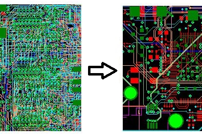
The above image shows several IC’s and a plethora of additional through-holes competing with several layers of routing, followed by a reduction of complexity as a result of shifting MUXing circuitry and relays to a module. Now the instrument-to-DUT routing is no longer competing with the component-to-component routing. High density routing also increases noise, trace length and in may cause competing traces to decrease in width. Other benefits may include:
Increased Site Count
Loadboard Cost-Downs
Design Cycle Contraction
Rapid Repair/Replacement of Damaged Circuitry
We offer several standard solutions including:
Relays (Bulk, MUX or TREE formats)
Load Switching
PhotoMOS Switching
Utility Drivers
FPGA / Microcontrollers
DAC/ADC Circuits
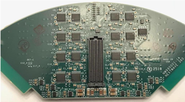
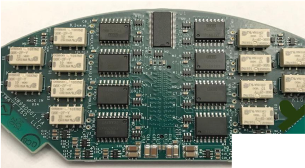
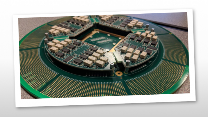
The following pictures are examples of actual solutions in production today. With the ability to move circuitry off the main board and onto these modules, our customer was able to increase their test site count from 16 site to 32. With NextWave's expertise in interface hardware - design & layout, in combination with our modules solutions, and the innovative P2 Interposer (pitch translation), NextWave can help you increase your test output and help you develop interface hardware with lower overall complexity, lowering its cost and increasing its manufacturability.
Give us a call, and our engineers will work closely with you to develop a custom solution that closes your test gaps and reaches your test objectives.

