Pitch Translation - The NextWave 360 Approach
Pitch Translation - Current Situation:
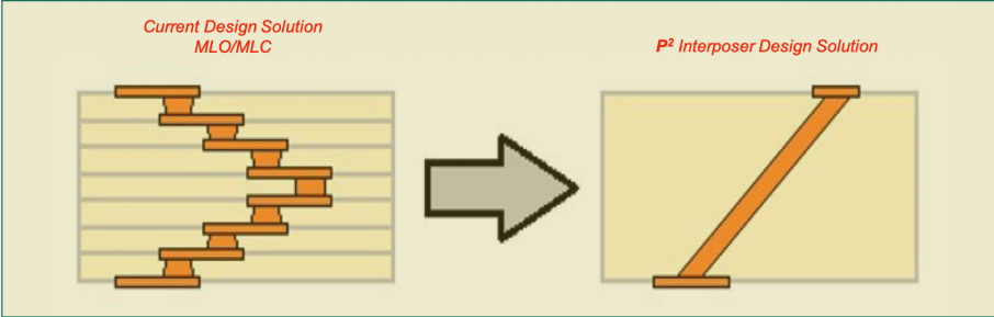
A common problem in the Semiconductor test interface world is the continuously shrinking package sizes and pitches required in designing and building test interface hardware. It has become more difficult for semiconductor manufacturers to test their devices with low cost and timely interface solutions. The challenges brought on by these tighter pitch devices have been passed on to the hardware design engineer and the FABs to work out solutions. While there are currently work around types of solutions to pitch translation, they are less than ideal from a cost, schedule and DFM (design for manufacturing) perspective. With these current solutions, a mother PCB will have a design with a higher more complex layer count, and require an MLO/MLC board often with blind/buried vias, micro/laser vias and many layers. Often times MLO/MLC solutions combined with the mother board are fraught with issues such as increasing complexity in the board, reliability issues, yield loss, increased manufacturing costs, long schedule times, design schedule gating, and even a risk that the solution may not be manufacturable at all. Even if the solution is manufacturable, very few FABs around the world have this level of capability, reducing available FAB options. The Engineers at NextWave 360 are very experienced in this industry and having lived through these problems, have developed innovative solutions that will change the way test interface hardware is designed in the future.
The NextWave 360 Approach:
NextWave 360 is dedicated to helping customers solve their most complex test interface challenges. To tackle the DFM issues previously described, NextWave 360 Engineers have developed the revolutionary P2 Interposer (Patent Pending # 62774910). This fantastic innovation is making an impact in the Semiconductor Interface application world. The P2’s advantage in the market is in its simplicity of design. This innovation offers significant cost and schedule improvement over current MLO/MLC solutions. The P2 Interposer significantly drives down layer count in the mother board, and due to the pitch translation qualities, simplifies the design and manufacturing of the boards such that more FABs are capable of manufacturing them. This improved DFM simplicity drives up quality and reduces yield loss and costly waste. Since the design of the P2 Interposer itself can be completed very quickly, it does not gate the design of the mother board, which reduces the total design cycle. While most MLO/MLC solutions are permanent fixtures on these interface boards, the P2 Interposer, with attached elastomer pins, can be easily installed and removed to or from the mother board right on the test floor by the engineer. It is that easy to install! This allows for simple repair and saves the mother board from potential scrap once the MLO/MLC starts to fail.
What is the P2 Interposer?
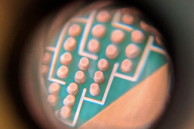
The P2 Interposer is an innovative space transforming solution, using continuous, straight through angled vias in a two-layer, monolithic substrate. This design and manufacturing approach provides the ability to transform the main board pitch ranges from 0.8 mm to a pitch of 0.15 mm, taking away the burden from the main board and is a viable solution across all tester manufacturers and platforms.
P2 Design, Manufacturing and Installation:
The overall process flow from capturing the design and shipping the interposers to the customer is currently about a 3-week turnkey process. The P2 Interposer is manufactured by taking the pitch translation design and adding the straight through angled vias, as designed, plating those vias and filling them using a conductive or non-conductive epoxy. In the finishing stages of manufacturing, the pads receive a typical plate-up including Nickel/Gold, as would any other PCB pad. Standard soldermasks and silkscreens are also available. The interposers are tested and visually inspected before moving on to shipment or pin assembly.
The P2 interposer is re-flow compatible for customers that prefer to add the interposer to the board during the component assembly process, however the preferred installation methodology is by utilizing elastomer pins. Before shipping, the elastomer pins would be added, and a compression stop provided. Installation can be done on-site by attaching to the board itself or held in place by the device socket attachment. Utilizing this installation method, the interposer can be added or removed from the board at any time, making it ideal for shipping to manufacturing test floors around the world.
Key P2 Attributes & Benefits:
- Pitch gain capability up to 400%
- 1 Mil/Linear Inch planarity
- Pitch capability as low as 0.15mm
- Socket/Probehead alignment within 10 microns
- Up to 25GHz of high-quality performance
- Characterized up to 10A continuous
- Design in as little as one day
- Delivery in as little as three weeks
- Easy on-site installation, via elastomer pins. Also Re-flow compatible
- Increases signal integrity, lowers layer count & reduces overall cost
- Allows for more FAB houses to compete for the business
- Removes barriers to DFM challenges, increasing FAB yield
- Reduces overall cost
- Completely tester agnostic
For more information, please contact US - https://nextwave-360.com/contact-us
Click Here to Open Our P2 Interposer Brochure

